


•rйgЈә2025-02-24 ҒнФҙЈәәП·КҫWhfw.cc ЧчХЯЈәhfw.cc ОТТӘјmеe

|
|

|
|
|
|
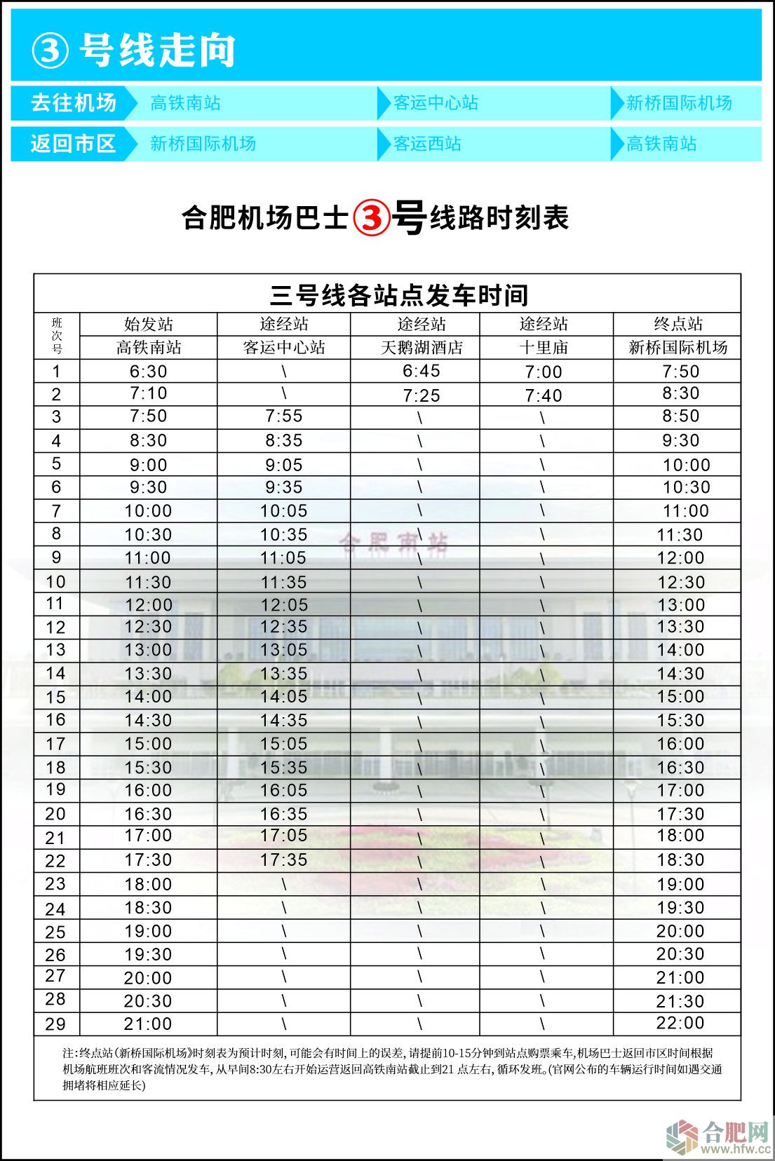
|
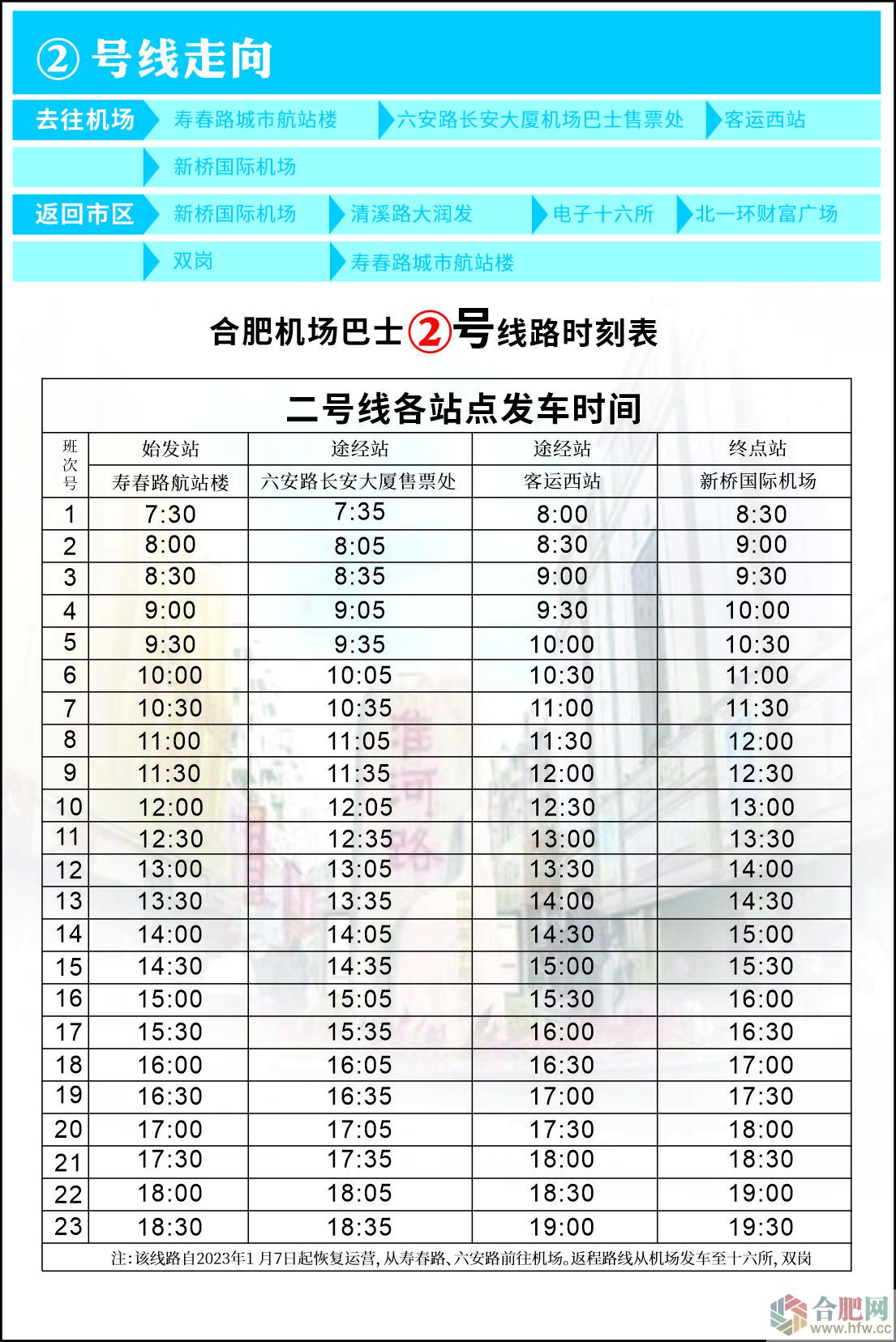
|
 |
¶МРЕтһЧCҙa ¶№°ь ҺЕ°ІПВЭd ДҝдӣҫW
Copyright © 2025 hfw.cc Inc. All Rights Reserved. әП·КҫW °жҷаЛщУР
ICPӮд06013414М–-3 №«°ІӮд 42010502001045